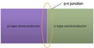
We can produce a single crystal with p-type semiconductor on one side and n-type on the other side as shown in figure above.
The border where the p-type and the n-type region meet is called the p-n junction.
Depletion Layer and Junction Voltage
At the p-n junction, electrons from the n-type semiconductor will be attracted to the holes in the p-type semiconductor.
As a result, the holes and the electrons at the p-n junction disappear, forming a layer called “depletion layer”.
At the same time, the p-type semiconductor becomes more negative whereas the n-type semiconductor becomes more positive.
This will result a potential difference across the p-n junction. This potential difference is called the junction voltage (or the barrier voltage).
The junction voltage will prevent the charge carrier from flowing across the depletion layer.
Forward Bias And Reverse Bias
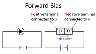
(figure 1)
The figure above shows a dc source across a diode. The negative source terminal is connected to the n-type material, and the positive terminal is connected to the p-type material.
This connection Figure is called forward bias.
Current flows easily in a forward-biased silicon diode.
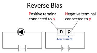
(Figure 2)
Turn the dc source around and you reverse-bias the diode as shown in Figure 2.
This time, the negative battery terminal is connected to the p side, and the positive battery terminal to the n side. This connection is called reverse bias.
Depletion Layer Widens
The negative battery terminal attracts the holes, and the positive battery terminal attracts the free electrons. Because of this, holes and free electrons flow away from the junction. Therefore, the depletion layer gets wider.