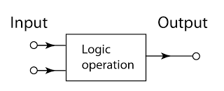
- Logic gates can be combined together to perform certain tasks.
- The output can be determined by constructing a truth table.
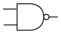
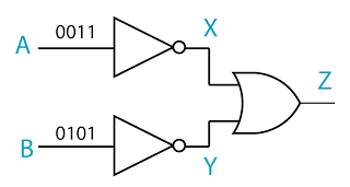
Example 1:
In the combination of logic gate above, find the outputs X, Y and Z of of the inputs A and B.
Answer:
In the combination of logic gate above, find the outputs X, Y and Z of of the inputs A and B.
Answer:
| INPUT | OUTPUT | ||||
| A | B | X | Y | Z | |
| 0 | 0 | 1 | 1 | 1 | |
| 0 | 1 | 1 | 0 | 1 | |
| 1 | 0 | 1 | 1 | 1 | |
| 1 | 1 | 0 | 0 | 0 | |
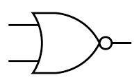
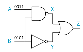
Example 2:
In the combination of logic gate above, find the outputs X, Y and Z of of the inputs A and B.
Answer:
In the combination of logic gate above, find the outputs X, Y and Z of of the inputs A and B.
Answer:
| INPUT | OUTPUT | ||||
| A | B | X | Y | Z | |
| 0 | 0 | 1 | 1 | 1 | |
| 0 | 1 | 1 | 0 | 1 | |
| 1 | 0 | 0 | 1 | 1 | |
| 1 | 1 | 0 | 0 | 0 | |
Example 3:
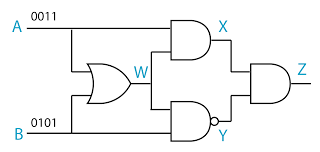
In the combination of logic gate above, find the outputs X, Y and Z of of the inputs A and B.
Answer:
In the combination of logic gate above, find the outputs X, Y and Z of of the inputs A and B.
Answer:
| INPUT | OUTPUT | |||||
| A | B | W | X | Y | Z | |
| 0 | 0 | 0 | 0 | 1 | 0 | |
| 0 | 1 | 1 | 0 | 0 | 0 | |
| 1 | 0 | 1 | 1 | 0 | 0 | |
| 1 | 1 | 1 | 1 | 0 | 0 | |
Example 4:
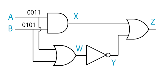
In the combination of logic gate above, find the outputs X, Y and Z of of the inputs A and B.
Answer:
In the combination of logic gate above, find the outputs X, Y and Z of of the inputs A and B.
Answer:
| INPUT | OUTPUT | |||||
| A | B | W | X | Y | Z | |
| 0 | 0 | 0 | 0 | 1 | 1 | |
| 0 | 1 | 1 | 0 | 0 | 0 | |
| 1 | 0 | 1 | 0 | 0 | 0 | |
| 1 | 1 | 1 | 1 | 0 | 1 | |