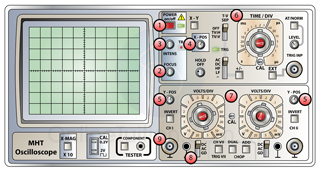
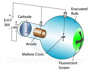
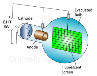
In a laboratory, a cathode ray oscilloscope can used to
- display different types of wave form.
- measure short time interval
- measure potential difference (as a voltmeter)
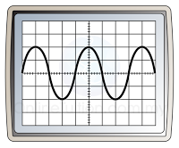
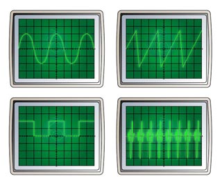
Displaying Wave Forms
- A cathode ray oscilloscope can be used to display different types of waveform by connecting a power supply to the Y-input.
- Figure below shows a few types of waveform displays on an oscilloscope.
Click on the links below for discussion about measuring short time interval and measuring potential difference
- Measuring Short Time Interval
- Measuring Potential Difference
Measuring Potential Difference
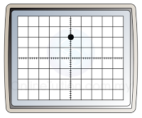
- In order to measure the potential difference, we need to move the bright spot to the centre before the Y-input is connected to any circuit.
- We also need to set the Y-gain. However, this can be adjusted later so that the signal can be fully displayed on the screen.
- The potential to be measured is then applied to the Y-plates via the Y-input terminals.
Measuring Potential Difference of a Direct Current
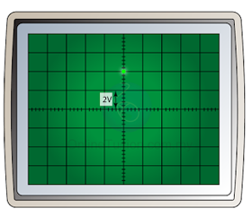
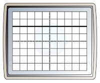
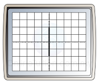
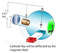
- The time-base is switched off. When a potential difference is applied to the Y-input, an electric field is set up between the plates. This will deflect the cathode ray either up or down.
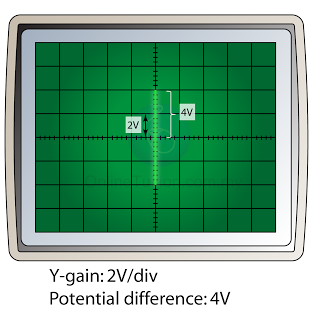
- The deflection of the electron beam by an electric field is proportional to the voltage applied. The reading of the voltage can be determined by referring to the Y-gain.
- For example, in the figure above, if the Y-gain is set to 2V per division (2V/div), then the reading of the potential difference is 4V.
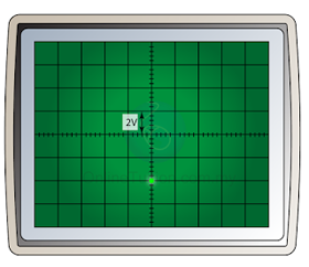
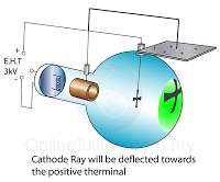
- If the terminal of the direct current is inverted, the bright spot will be deflected to the opposite side, as shown in the diagram below. The reading of the potential difference will remain the same (4V).
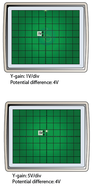
Effect of the Y-gain
Figure below shows the display of the CRO when the Y-gain is set to 1V/div and 5V/div respectively for a potential difference of 4V.
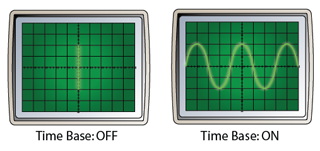
Effect of the Time Base
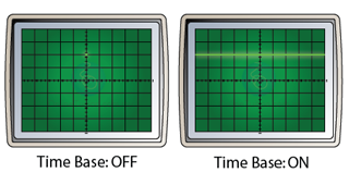
- The time base move the bright spot across the screen at a constant speed.
- Usually, the speed is very high. As a result, we are not able to see the motion of the bright spot, but a straight line across the screen.
- Figure below shows the display of a CRO when the time base is ON and OFF.
Measuring Potential Difference of an Alternating Current
- If an alternating current is connected to the Y-input, a changing potential difference will be applied between the Y-plates.
- The changing potential difference will move the bright spot up and down continuously.
- As a result, vertical straight line will form on the screen of the CRO. The reading of the potential difference can be determined by referring to the Y-gain.
- For example, for the diagram above, if the Y-gain is set to 2V/div, then the maximum potential difference (peak voltage) is 4V.
Effect of the Time Base
- If the time base is switched on, it will move the bright spot across the screen horizontally.
- The result of the vertical motion caused by the Y-plate and the horizontal motion caused by the time base is a sinusoidal wave form.
- Diagram below shows the CRO display when the time base is on and off.
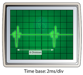
Measuring Short Time Interval
- A cathode ray oscilloscope can be used to determined the time interval between 2 pulses, even though the time interval is very small.
- Figure above shows 2 pulses on the screen of a cathode ray oscilloscope.
- If the time base is set to 2 ms/div, the time interval between the 2 pulses can be calculated as follow:
t = 6 x 2ms = 12 ms = 0.012s.